
NANOscientific
Forum Europe 2025
17 - 19 September, 2025 | Orsay, France
NANOscientific Forum Europe 2025
The NSFE is part of the NANOscientific Symposium Series a gloabl event series focused on advanced techniques in Atomic Force Microscopy (AFM), Imaging Spectroscopic Ellipsometry (ISE), and nanotechnology applications in material and life sciences.
NSFE2025 is designed for researchers, engineers, students, and industry professionals working in materials science, life sciences, and surface analysis. The symposium offers:
- Hands-on sessions with cutting-edge instruments
- Expert talks from leading scientists
- Networking opportunities with peers and innovators
The 8th edition of the NANOscientific Forum Europe will be held from September 17th - 19th, 2025 at the Laboratory of Solid State Physics (LPS), located in Orsay, France, approximately 25 km southwest of Paris. THe LPS is a research institute of Paris-Saclay University, affiliated with the National Center for Scientific Research (CNRS) as a joint research unit (UMR 8502).
This year’s host is Dr. Stanislas Rohart, a specialist in magnetic imaging (STM and MFM) and micromagnetism. He pioneered investigations on the Dzyaloshinskii-Moriya interaction in ultrathin films and its consequences on chiral domain walls and skyrmions. His present research mostly focuses on magnetic skyrmions in ferromagnetic and magnetically compensated films.
The scientific focus this year will include Magnetic Force Microscopy and 2D Materials, as well as new developments and innovative methods in nanotechnology and correlative microscopy. Attendees will have the opportunity to hear from and engage with distinguished keynote speakers, such as our host Stanislas Rohart and Dr. Rebeca Ribeiro-Palau from C2N, among others. Explore the full program.
The event will extend beyond scientific discussions and offer participants many networking opportunities, such as the conference dinner on a scenic Seine river cruise and the social event at a local winery.
As in previous years, there will be Hands-on Sessions on Park Systems tools, showcasing basic and advanced measuring techniques, as well as tips and tricks on how to obtain stunning AFM and ISE data:
See nanoscale characterization redefined with Park’s FX200 IR AFM. From high-precision PiFM-based IR spectroscopy to automated laser alignment and advanced AFM modes, this system delivers unmatched insight into nanomechanical, electrical, and thermal properties.
Experience how Ellipsometry visualizes buried interfaces, anisotropic structures, and fluid interlayers in real time, and bring your own samples to see them come alive under the lens of Mueller Matrix Ellipsometry. And much, much more.
Park Systems Instruments, you will get to see live:
- FX200 IR AFM - integrating nanoscale infrared (IR) spectroscopy with atomic force microscopy (AFM) to deliver advanced chemical and materials characterization.
- FX40 AFM - the automatic AFM streamlines data collection, research workflows, and data publication, empowering accelerated scientific progress and discovery.
- NX10 AFM - the premier choice for cutting-edge materials science research that provides ease of use with high-resolution capabilities.
- Accurion Simon - combining the sensitivity of thickness and refractive index measurements with the imaging capabilities of microscopy.
- Reflection DHM R 2200 with stroboscopic unit - recording holograms produced by the interference between the beam transmitted through the sample, and a reference beam generated inside of the microscope.
Program & Speaker
08:30 - 09:00
Registration & Meet and Greet
09:00 - 09:45
Welcome to the NSFE2025
09:45 - 09:50
Electronic Properties of 2D Devices
09:50 - 10:15
Nano-infrared visualization and tuning of propagating polaritons in free-standing oxide membranes
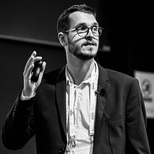
Assist. Prof. Alexander McLeod
Assist. Prof. Alexander McLeod
10:15 - 10:45
Coffee Break
14:00 - 15:00
Lunch
10:45 - 11:10
Exploring ABC-stacked graphene domains in untwisted epitaxial graphene
Dr. Martin Rejhon
11:10 - 11:35
High-throughput correlated microscopy and automated device integration of 1D and 2D materials
Dr Jack Alexander-Webber
11:35 - 11:50
Correlative metrology for the stufdy of the physico-chemical properties of graphene oxide during its reduction
Lydia Chibane
11:50 - 12:05
Nanoplast experimental set-up
12:05 - 13:35
Lunch
13:35 - 13:40
Probing Electrochemical Features via SPM
13:40 - 14:05
Electrochemical Strain Wave Microscopy for Mapping Mixed Ionic-Electronic Transport
Prof. Dr. Tobias Cramer
14:05 - 14:30
Scanning Probe Microscopy for Electrochemical Research by Park Systems
Dr. Alexander Klasen
14:30 - 14:45
Modulated Electrochemical AFM for Nanoscale Analysis of Ion Intercalation in Battery Materials
Nikolas Franke
14:45 - 15:00
Wrap Up Day 1
15:00 - 15:30
Coffee Break
15:30 - 17:00
Hands-on Sessions
17:00 - 18:00
Poster Session
19:00 - 23:00
Conference Dinner
09:00 - 09:10
Spintronics and Magnetic Imaging
09:10 - 09:55
Probing Magnetic Skyrmions Dynamics in Ferromagnetic and Synthetic Antiferromagnetic Films
Dr. Stanislas Rohart
09:55 - 10:25
Coffee Break
10:25 - 10:50
Scanning probe magnetic microscope with magnetoresistive magnetic sensors
Dr. Aurélie Solignac
10:50 - 11:15
Illustration of the trilemma Sensitivity – Spatial Resolution – Probe response in Magnetic Force Microscopy
Dr. Olivier Fruchart
11:15 - 11:30
tbc
12:30 - 12:35
Advances in SPM - Combining Correlative Techniques
12:35 - 13:00
Examples of Infrared Nano-Spectroscopy and Imaging in Soft Matter: Polymers in Porous Materials, Thin Film Coatings in Battery Materials and Solar Cells
13:00 - 13:25
Interface Characterization of Sulfonated Cellulose Nanocrystal/sPEEK Nanocomposites via Photo-Induced Force Microscopy
13:25 - 13:50
Thermal characterization at the micro- and nanoscale
Nolwenn Fleurence
13:50 - 14:15
Nanomechanical Characterization of Organic Molecular Semiconductors via AFM
Ki-Hwan Hwang
14:15 - 14:40
3D time-resolved topography and MEMS analysis by DHM
14:40 - 15:15
Sponsor talks & Wrap up day 2 & Group Photo
15:15 - 15:45
Coffee Break
15:45 - 17:00
Hands-on Sessions
17:30 - 21:30
Social Event
09:00 - 09:10
News and Trends in Imaging Techniques
09:10 - 09:55
Twist-Angle-Controlled Anomalous Gating in Bilayer Graphene/BN Heterostructure
Dr. Rebeca Ribeiro-Palau
12:00 - 13:30
PFM & cAFM – Indispensable Tools when Engineering 2DEGs into Wide-Bandgap Semiconductors
10:20 - 10:50
Coffee Break
10:50 - 11:15
Deciphering Electrical Bistability in Nanocomposite by Electrostatic Force Microscopy
11:15 - 11:40
Advanced Nanoelectrical Characterization of Nanowires
11:40 - 11:55
Multi-scale characterization of a functionalized substrate using advanced surface analysis techniques
11:55 - 12:10
A study on the morphological, mechanical and electrostatic properties of transferred single crystalline La0.7Sr0.3MnO3 freestanding membranes
Markos Paradinas
12:10 - 12:25
"A Multiscale Approach to Optical Surface Characterization: Integrating AFM and Optical Methods
12:25 - 12:40
A novel experimental method to investigate mechanism of water capillary condensation
12:40 - 13:15
Closing Ceremony
13:15 - 14:15